Probe Stations
The term ‘Probe Station’ covers a wide range of devices used to position analytical or test probes for non-destructive electrical testing at various locations on test samples. The examples here show a wide variety of different sizes and types available for use in semiconductors, material science, physics, optics, and MEMS. All have been tailored specifically for the end user’s unique access, range, temperature and test requirements. These are intended to show the range of possibilities from the MTS custom design and fabrication shop and the list is hardly exhaustive. Please contact us to discuss your particular needs.
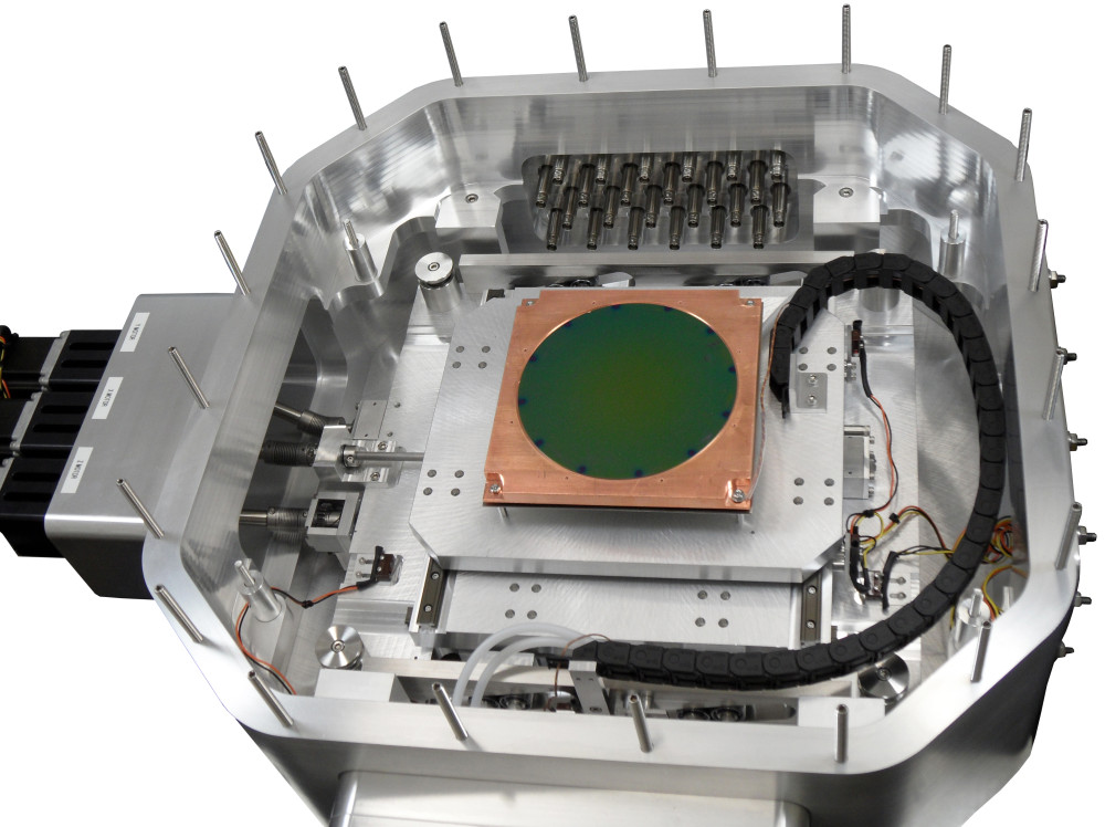
Large Sample Size – 6″ (150 mm)
- Shown with cover removed
- Full access to entire wafer surface
- ±3″ (±765 mm) XY travel
- 0.5″ (12.5 mm) Z travel
- Computerized motion control
- Cooling to -40C
- 48 instrumentation feedthroughs
- 1000X trinocular Microscope (not shown)
- Integrated multi-circuit probe card mounting
- Individual vacuum-compatible scanning probes
- Vacuum level to 10-6 torr
- Additional instrumentation ports
- High precision positioners <0.0001″ (<2µ)
